- 您现在的位置:买卖IC网 > Sheet目录17352 > AD588JQ (Analog Devices Inc)IC VREF SERIES PREC ADJ 16-CDIP
�� ��
��
��AD588�
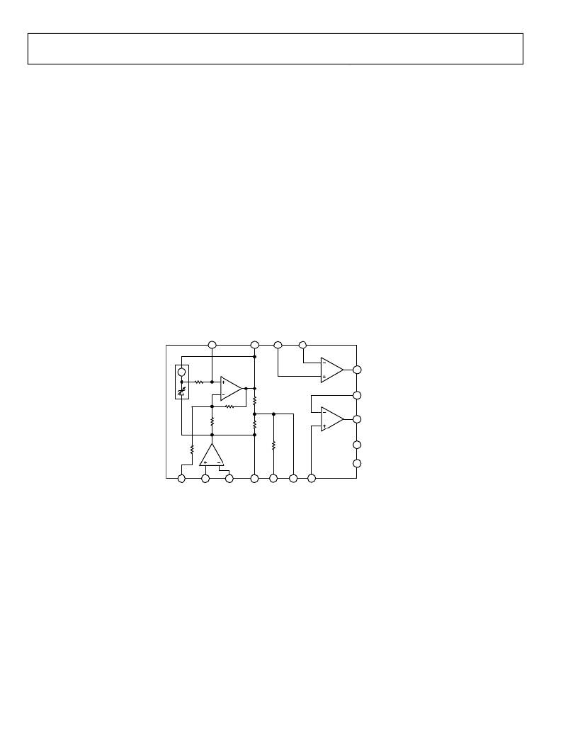
�THEORY� OF� OPERATION�
�The� AD588� consists� of� a� buried� Zener� diode� reference,�
�amplifiers� used� to� provide� pin� programmable� output� ranges,�
�and� associated� thin-film� resistors,� as� shown� in� Figure� 3.� The�
�temperature� compensation� circuitry� provides� the� device� with�
�a� temperature� coefficient� of� 1.5� ppm/°C� or� less.�
�Amplifier� A1� performs� several� functions.� A1� primarily� acts� to�
�amplify� the� Zener� voltage� from� 6.5� V� to� the� required� 10� V�
�output.� In� addition,� A1� provides� for� external� adjustment� of� the�
�10� V� output� through� Pin� 5,� GAIN� ADJ.� Using� the� bias�
�compensation� resistor� between� the� Zener� output� and� the�
�noninverting� input� to� A1,� a� capacitor� can� be� added� at� the�
�NOISE� REDUCTION� pin� (Pin� 7)� to� form� a� low-pass� filter� and�
�reduce� the� noise� contribution� of� the� Zener� to� the� circuit.� Two�
�matched� 10� k� nominal� thin-film� resistors� (R4� and� R5)� divide�
�the� 10� V� output� in� half.� Pin� V� CT� (Pin� 11)� provides� access� to� the�
�center� of� the� voltage� span� and� BAL� ADJ� (Pin� 12)� can� be� used�
�for� fine� adjustment� of� this� division.�
�Ground� sensing� for� the� circuit� is� provided� by� Amplifier� A2.� The�
�noninverting� input� (Pin� 9)� senses� the� system� ground,� which� is�
�transferred� to� the� point� on� the� circuit� where� the� inverting� input�
�(Pin� 10)� is� connected.� This� can� be� Pin� 6,� Pin� 8,� or� Pin� 11.� The�
�output� of� A2� drives� Pin� 8� to� the� appropriate� voltage.� Thus,� if�
�Pin� 10� is� connected� to� Pin� 8,� the� V� LOW� pin� is� the� same� voltage� as�
�the� system� ground.� Alternatively,� if� Pin� 10� is� connected� to� the�
�V� CT� pin,� it� is� a� ground;� and� Pin� 6� and� Pin� 8� are� +5� V� and� ?5� V,�
�respectively.�
�Amplifier� A3� and� Amplifier� A4� are� internally� compensated� and�
�are� used� to� buffer� the� voltages� at� Pin� 6,� Pin� 8,� and� Pin� 11,� as� well�
�as� to� provide� a� full� Kelvin� output.� Thus,� the� AD588� has� a� full�
�Kelvin� capability� by� providing� the� means� to� sense� a� system�
�ground� and� provide� forced� and� sensed� outputs� referenced� to�
�that� ground.�
�Note� that� both� positive� and� negative� supplies� are� required� for�
�operation� of� the� AD588.�
�NOISE�
�REDUCTION�
�7�
�V� HIGH�
�6�
�A3� IN�
�4�
�A3� OUT�
�SENSE�
�3�
�R� B�
�A1�
�R1�
�R4�
�A3�
�1�
�14�
�A3� OUT�
�FORCE�
�A4� OUT�
�SENSE�
�R2�
�R5�
�A4�
�15�
�A4� OUT�
�FORCE�
�R3�
�A2�
�R6�
�AD588�
�2�
�+V� S�
�16�
�–V� S�
�5�
�9�
�10�
�8�
�12�
�11�
�13�
�GAIN�
�ADJ�
�GND� GND�
�SENSE� SENSE�
�V� LOW�
�BAL�
�ADJ�
�V� CT�
�A4� IN�
�+IN�
�–IN�
�Figure� 3.� AD588� Functional� Block� Diagram�
�Rev.� L� |� Page� 6� of� 20�
�发布紧急采购,3分钟左右您将得到回复。
相关PDF资料
A9BAA-0506F
FLEX CABLE - AFF05A/AF05/AFE05T
RE-2412S/H
CONV DC/DC 1W 24VIN 12VOUT
ESM06DRMN
CONN EDGECARD 12POS .156 WW
AS1323-30 EB
BOARD EVAL AS1323-30
AS1323-27 EB
BOARD EVAL AS1323-27
RE-2409S/H
CONV DC/DC 1W 24VIN 09VOUT
EGM06DRMN
CONN EDGECARD 12POS .156 WW
LQW2UAS12NJ00L
IND 12NH 1000MA SRF 3300MHZ 1008
相关代理商/技术参数
AD588KQ
功能描述:IC VREF SERIES PREC ADJ 16-CDIP RoHS:否 类别:集成电路 (IC) >> PMIC - 电压基准 系列:- 标准包装:2,000 系列:- 基准类型:旁路,可调节,精度 输出电压:1.24 V ~ 16 V 容差:±0.5% 温度系数:- 输入电压:1.24 V ~ 16 V 通道数:1 电流 - 阴极:100µA 电流 - 静态:- 电流 - 输出:20mA 工作温度:-40°C ~ 85°C 安装类型:通孔 封装/外壳:TO-226-3、TO-92-3(TO-226AA)成形引线 供应商设备封装:TO-92-3 包装:带卷 (TR)
AD588SD
制造商:未知厂家 制造商全称:未知厂家 功能描述:Voltage Reference
AD588SD/883B
制造商:未知厂家 制造商全称:未知厂家 功能描述:Voltage Reference
AD588SE
制造商:Rochester Electronics LLC 功能描述:- Bulk
AD588SE/883B
制造商:Analog Devices 功能描述:V-Ref Programmable ±5V/±10V 20-Pin LCC Tube
AD588SQ
制造商:Rochester Electronics LLC 功能描述:IC - PROGRAMMABLE V REF. - Bulk
AD588SQ/883B
制造商:Rochester Electronics LLC 功能描述:IC - PROGRAMMABLE V REF. - Bulk
AD588TD
制造商:未知厂家 制造商全称:未知厂家 功能描述:Voltage Reference